
KiCAD PCB Viewer
KiCAD PCB Viewer generates an estimated $90–$2k/month in revenue from 100–600 downloads/month on the App Store, according to AppCurrents estimates (updated 2026-10-02).
| Est. revenue / month | $90–$2k |
|---|---|
| Est. downloads / month | 100–600 |
| Estimate confidence | medium |
| Pricing | Paid $1.99 |
| Rating | 1.00 ★ (3 ratings) |
| Category | Graphics & Design |
| Best chart rank | #57 Graphics & Design Paid |
| Released | 29.06.2023 |
| App last updated | 28.09.2026 |
| Platform | iOS |
Modeled monthly estimate · rating velocity · medium confidence
About
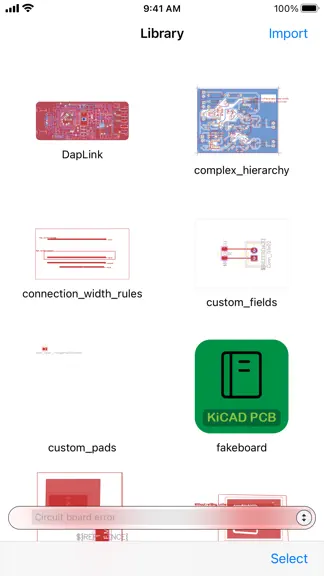
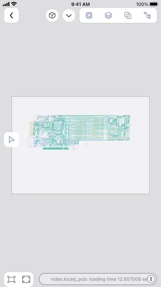
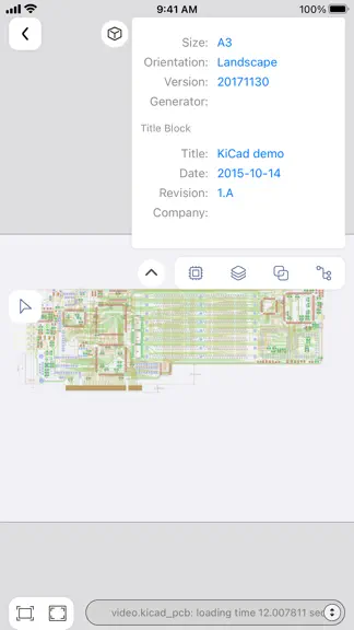
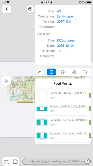
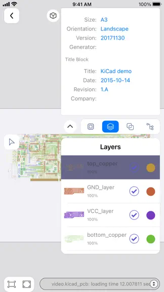
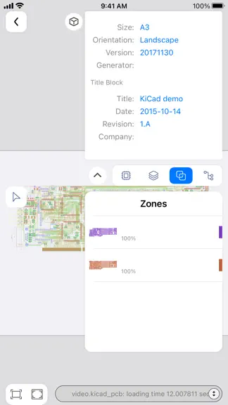
This is a lightweight APP for viewing KiCAD 3 - 10 generated pcb files in a mobile environment. No matter what questions, opinions or ideas you have, you can send an email to [email protected] . KiCAD PCB Viewer is a highly professional tool developed specifically for viewing and reviewing PCB design files generated by KiCAD. The tool integrates an advanced graphical interface that allows users…
Trends & analysis
Chart rank trend
US · categoryWhy it's surfacing
Scout 15Ratings & velocity
★ 0 in windowRating distribution
0% positive · 3 ratingsGeographic reach
best rank · 1 storefrontRevenue & downloads trend
ARPU $1Update history
9 updates tracked- v1.3.93d ago
Thank you for your feedback! New features in this release: New: 3D mode reconstructs silkscreen text into smooth-rendered line capsule primitives and supports dashed line styles; New: 3D mode enables rendering of blind, buried, and through-hole via wall metallization with copper plating, and introduces radial inward compensation for via diameters; New: 3D mode supports high-fidelity rendering of footprint-level copper shapes (fp_poly, fp_line, fp_text); New: 3D mode supports automatic edge drilling clipping and precise contour trimming for non-circular slot holes; Improved: Expression parsing kernel now uses thread-safe high-precision floating-point conversion, significantly enhancing large file loading speed; Improved: Reconstructed layer alias mapping system enables O(1) fast lookup across the entire footprint lifecycle and improved layer organization; Improved: Decoupled document loading from thumbnail generation, enabling asynchronous background rendering of thumbnails; Improved: Enhanced grid triangulation algorithm strengthens area and perimeter conservation checks for complex polygon topologies; Fixed: Routing traces and arcs are reconstructed as continuous closed capsule geometries, eliminating endpoint voids via nonzero winding number detection; Fixed: Resolved issue where pad and copper side walls in 3D mode appeared completely black under PBR lighting due to missing normal vectors; Fixed: Addressed mesh generation and triangulation defects at keyhole bridging notches between solid silkscreen and copper polygons; Fixed: Fixed problem where overlapping pads or adjacent SMD pads could occlude through-holes during inter-layer penetration; Fixed: Resolved occasional anomalies where pad geometry cache and layer state became desynchronized during undo/redo operations.
- v1.3.813d ago
Thank you for your feedback! New features in this release: New: 3D mode reconstructs silkscreen text into smooth-rendered line capsule primitives and supports dashed line styles; New: 3D mode enables rendering of blind, buried, and through-hole via wall metallization with copper plating, and introduces radial inward compensation for via diameters; New: 3D mode supports high-fidelity rendering of footprint-level copper shapes (fp_poly, fp_line, fp_text); New: 3D mode supports automatic edge drilling clipping and precise contour trimming for non-circular slot holes; Improved: Expression parsing kernel now uses thread-safe high-precision floating-point conversion, significantly enhancing large file loading speed; Improved: Reconstructed layer alias mapping system enables O(1) fast lookup across the entire footprint lifecycle and improved layer organization; Improved: Decoupled document loading from thumbnail generation, enabling asynchronous background rendering of thumbnails; Improved: Enhanced grid triangulation algorithm strengthens area and perimeter conservation checks for complex polygon topologies; Fixed: Routing traces and arcs are reconstructed as continuous closed capsule geometries, eliminating endpoint voids via nonzero winding number detection; Fixed: Resolved issue where pad and copper side walls in 3D mode appeared completely black under PBR lighting due to missing normal vectors; Fixed: Addressed mesh generation and triangulation defects at keyhole bridging notches between solid silkscreen and copper polygons; Fixed: Fixed problem where overlapping pads or adjacent SMD pads could occlude through-holes during inter-layer penetration; Fixed: Resolved occasional anomalies where pad geometry cache and layer state became desynchronized during undo/redo operations.
- v1.3.621d ago
Thank you for your feedback! New features in this release: New: Support for parsing and rendering rounded corners on rectangular primitives; New: Full 3D support for F.Cu/B.Cu top/bottom copper layer text, polygonal and rectangular geometry rendering; New: 3D mode now supports precise via drilling for blind and buried vias based on layer span; New: 3D silkscreen text is now represented using segmented capsule geometries, enabling complete rendering of multi-stroke and dashed styles in Hershey vector fonts; New: 3D mode supports boundary clipping and adaptive drilling for drill holes intersecting board edges; Fixed: Routing and arcs are reconstructed as continuous closed capsule geometries, eliminating endpoint gaps caused by non-zero winding numbers; Fixed: Elliptical and slot-shaped holes use precise geometric Boolean clipping, ensuring perfect clearance between routing and drill holes without covering them; Fixed: Improved 3D rendering of bottom-layer thermal pads, solder mask clearances, and mirrored characters; Fixed: Enhanced thread-safe background processing model based on main-thread snapshots and frequent cancellation checks, eliminating multi-threading race conditions; Fixed: Overlapping pads and vias are now built with independent nodes and merged once, preventing unwanted hollowing due to global Even-Odd rules; Fixed: Polygonal copper hole detection upgraded to odd-even parity, accurately supporting embedded islands and hollowed-out copper areas; Fixed: Resolved conflicts in project file build dependencies and UUID collisions; Fixed: Addressed issues where pad coordinates and attributes were not properly synchronized during undo/redo operations; Fixed: Corrected incorrect solid copper rendering for unfilled copper pours; Fixed: Resolved triangulation crashes and copper pour loss caused by overlapping micro-spacing cuts.
- v1.3.51mo ago
Thank you for your feedback! New features in this release: New: Network floating panel now supports real-time network search filtering and fully displays design rule parameters of the corresponding network category. New: Support for parsing and rendering new primitives in KiCad 7–10, including tables, barcodes/QR codes, alignment targets, reference points, and grouped containers. New: Support for cross-layer parsing and rendering of multi-layer copper pours and keepout areas. New: Support for parsing rectangular primitive corner radii and rendering rounded corners. Improved: Enhanced interaction experience for footprint and layer pop-up panels; selected items can be deselected by clicking again. Improved: Enhanced modern parameter parsing for board-level design configuration. Improved: Unified parsing architecture with cleanup of deprecated splitting logic. Improved: Standardized unique identifiers for primitives to support multi-attribute parsing with compatibility. Fixed: Resolved conflicts between project file build dependencies and UUIDs.
- v1.3.41mo ago
Thank you for your feedback! New features in this release: New: Support net class rule parsing, including trace width, clearance, via sizes, and differential pair design rules; New: Nets floating panel now supports real-time search filtering and full display of design rule parameters for each net class; Improved: Enhanced interaction in Footprints and Layers floating panels, allowing selected items to be deselected by tapping again; Improved: Optimized initial Layers panel state by removing the default layer selection; Improved: Multilingual localization support for nets and design rules.
KiCAD PCB Viewer — FAQ
How much money does KiCAD PCB Viewer make?
According to AppCurrents estimates, KiCAD PCB Viewer generates approximately $90–$2k per month (medium confidence), modeled from its the App Store chart performance, rating velocity, and monetization signals.
How many downloads does KiCAD PCB Viewer get?
KiCAD PCB Viewer sees an estimated 100–600 downloads per month on the App Store, per AppCurrents modeling.
Is KiCAD PCB Viewer free?
KiCAD PCB Viewer is a paid app priced at $1.99 on the App Store.
What is KiCAD PCB Viewer's rating?
KiCAD PCB Viewer holds a 1.00-star average from 3 ratings on the App Store. It currently ranks #57 on the Graphics & Design paid chart.
When was KiCAD PCB Viewer released?
KiCAD PCB Viewer launched on the App Store on 29.06.2023. Its latest version shipped 28.09.2026.
Apps like KiCAD PCB Viewer
See all alternatives → ProcreateGraphics & Design · $300k–$5.0M/mo
 Reface: AI Face Swap & EditorGraphics & Design · $270k–$1.5M/mo
 AI Maker: Photo Video FiltersGraphics & Design · $240k–$1.3M/mo
 Nomad SculptGraphics & Design · $100k–$1.7M/mo
 ThemePack: Widgets & WallpaperGraphics & Design · $160k–$850k/mo
 Artmate: Drawing TogetherGraphics & Design · $140k–$790k/mo